










Today, let's delve into the field of optical packaging and uncover the secrets behind the packaging of optoelectronic sensors! In the world of optical packaging, precision is the ultimate goal we always pursue, and we strive to achieve ultimate optimization for every component and every step. Please watch the video explanation~

Perfect light path, challenging the problem of light leakage
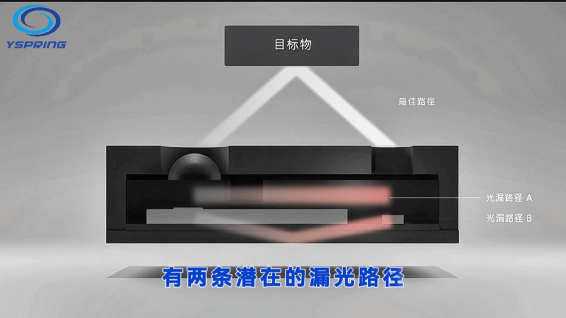
The light emitted by the sensor will be transmitted through the lens to the target object, and then reflected back into the receiver. This light path is the perfect light receiving and emitting path we want to achieve. But in this process, there are two potential light leakage paths that are like "little monsters" hidden in the dark, which can interfere with the accuracy of the sensor, so we must find ways to effectively eliminate them.
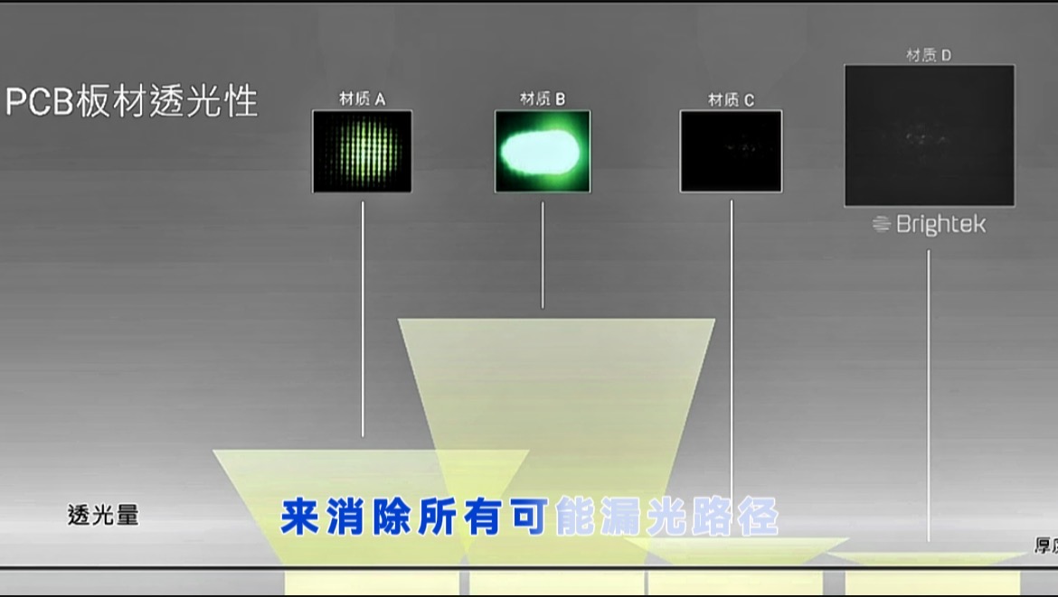
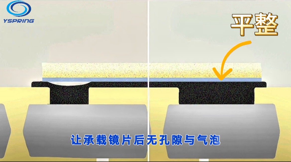
In the selection of the carrier board, we decisively chose opaque materials to eliminate all possible light leakage paths from the source. Moreover, in the bottom ink processing stage, we will make the chip flat, so that there will be no pores or bubbles after carrying the chip, greatly improving the overall adhesion and stability. This design is like building a dedicated "highway" for light, ensuring the correct transmission of light and reducing unnecessary light crosstalk.
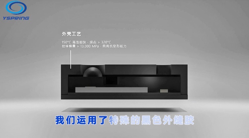
Not only that, we also use special black outer sealing glue and shell, which act like loyal "guards", highly blocking the crosstalk reaction between light and reception, allowing light to obediently move along the designed optical path without affecting the sensitivity of the sensor.
Solid crystal process, precision determines efficiency
After optimizing the external design, the internal solidification technology is crucial. The accuracy of solidification directly affects the efficiency of light emission and reception. And our solidification process has achieved a very high level of precision, ensuring that the installation angle and position of the chip are in the optimal state.
With this exquisite solidification process, we have successfully increased the light harvesting efficiency to over 80%! Moreover, we also achieve miniaturized packaging manufacturing by reducing glue overflow, which is the foundation for achieving excellent optical design.
Lens processing, details achieve precision
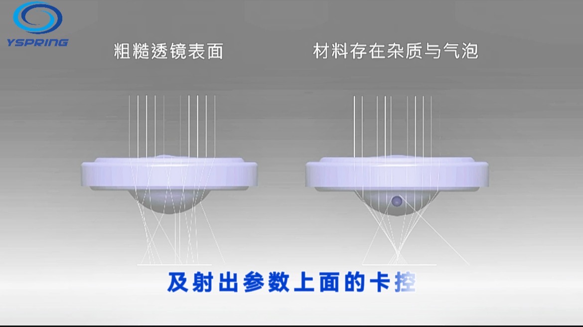
In addition to the solidification process, the processing quality of the upper lens and the selection of high temperature resistant materials are also another important factor affecting optical accuracy. The roughness and smoothness of the lens surface, like the "appearance" of the lens, directly affect the refraction and focusing effect of light.
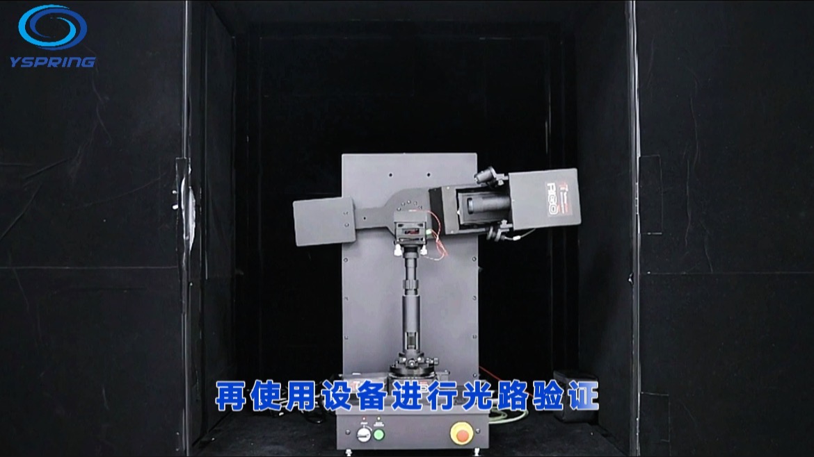
We strictly control the selection of materials and injection parameters in order to reduce the impact of material impurities and bubbles on the optical path. Finally, professional equipment is used for optical path verification to ensure the accuracy of the optical transmission and reception process, allowing the actual results to perfectly match the optical simulation.
Remarkable achievements, meeting diverse needs
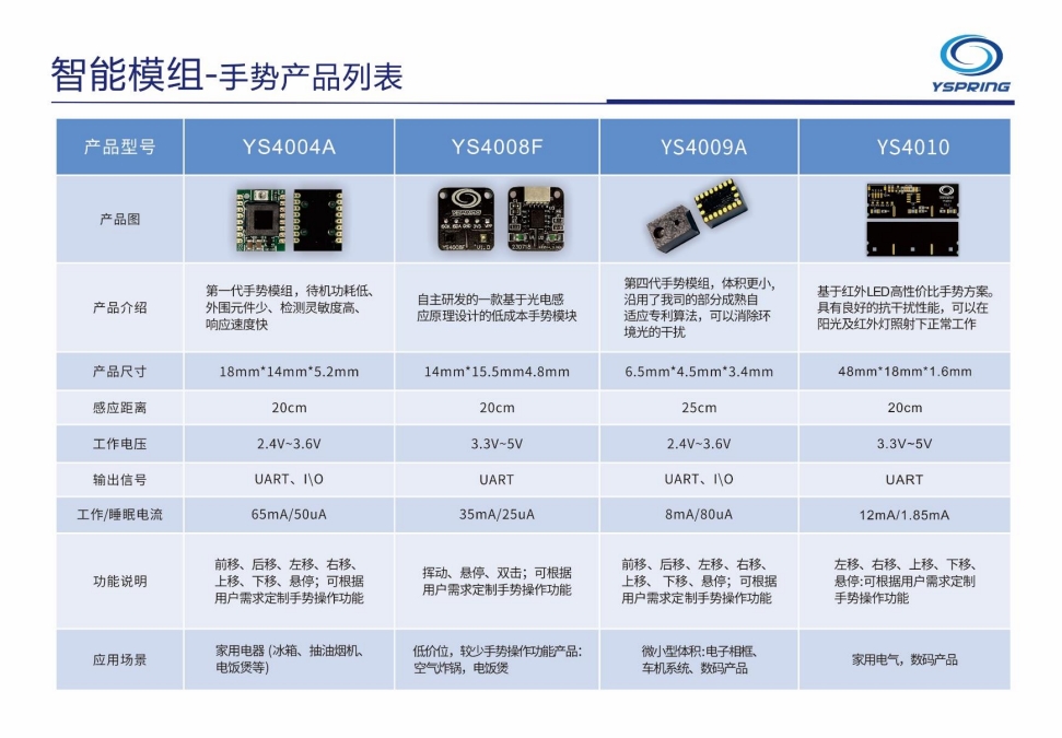
Through this series of design experience and precise process technology, we have successfully advanced the luminous efficiency to an ideal level close to 100%! With the help of advanced optoelectronic packaging technology, YSPRING has created a series of gesture control modules such as 4004, 4006, 4008, 4009, etc. These modules are like "magic assistants" that can meet the application needs of various industries. If you are interested, you can call our sales hotline (0755-86217885)
Your needs are the driving force behind our progress! In the future, we will continue to explore the path of optical packaging and bring more excellent products to everyone!


0755-86227153


